How I made my first PCB, screwed up, and fixed it
A month ago or so I was asked by a relative to make a voltage regulator from 12VDC to 5VDC for charging a USB device like a smartphone from a motorcycle battery (this was the intended usage). Now I know you can find these commercially for a few dollars, but I thought it would be a good opportunity to learn how to design printed circuit boards.
The exact user requirements were:
- it should take ~12VDC as input voltage, in other words 9VDC - 15VDC;
- it should output 5V on a USB plug that a device can be connected to;
- the USB plug should appear as a (fast) charging port to the device;
- an indicator LED should light on whenever a device is connected;
- or, failing that, at least when the regulator is powered on.
Design
The first question I asked myself was, how do I make the device appear as a charging port? This is actually a tricky question, but for most non-Apple smartphones out there, the correct way to signify this is to short the two data pins together. Easy. You can tell when this happens as the smartphone will report that it is e.g. “charging (AC)” instead of “charging from USB”.
For Apple smartphones you are out of luck as they use their own proprietary charging schemes to force people to buy Apple chargers. Some people have reverse-engineered this and produced universal chargers that work for every device, but in this case it was unnecessary as I only needed to support Android devices.
I decided to use a switching voltage regulator because a linear voltage regulator is inappropriate in this situation: 5V and 12V are quite far apart and with a maximum power output of around 7.5W, the low efficiency of linear regulators would require a heatsink to be installed. I decided to go with the ADP2303ARDZ-5.0-R7. This is a fixed 5-volt output model of the ADP2302/ADP2303 switching regulator family from Analog Devices.
Being a switching regulator, it requires at least an inductor, a flyback diode and some capacitors as external components to complete it. The nice thing about this component is that it has a fairly complete datasheet which includes not only a diagram of how to wire it up and rationale for the different configurations suggested, but it also suggests actual parts to use for the external components! This is what led me to choose this part despite it plus the necessary components quickly adding up in cost; more manufacturers should put such effort into their datasheets.
I eventually went with the circuit schematic below. The voltage regulation circuit is entirely lifted from the datasheet as I didn’t want to take risks, and the op-amp is a comparator meant to sense a current sensing resistor (R1).
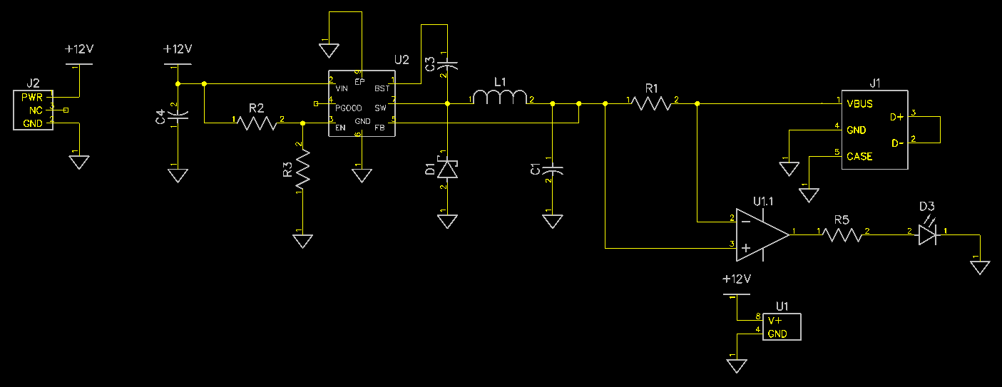
Schematic for the USB charging port.
For the current sense comparator I went with the TLC3702IDR for the main reason that according to its datasheet it can source up to 20 milliamps, which means it can drive an indicator LED by itself without needing a transistor. The idea here is that there should only be a voltage drop across R1 if a load exists between VBUS and GND, so the LED should only turn on when a device is connected to the USB jack.
After doing some manual routing the PCB looked like this:
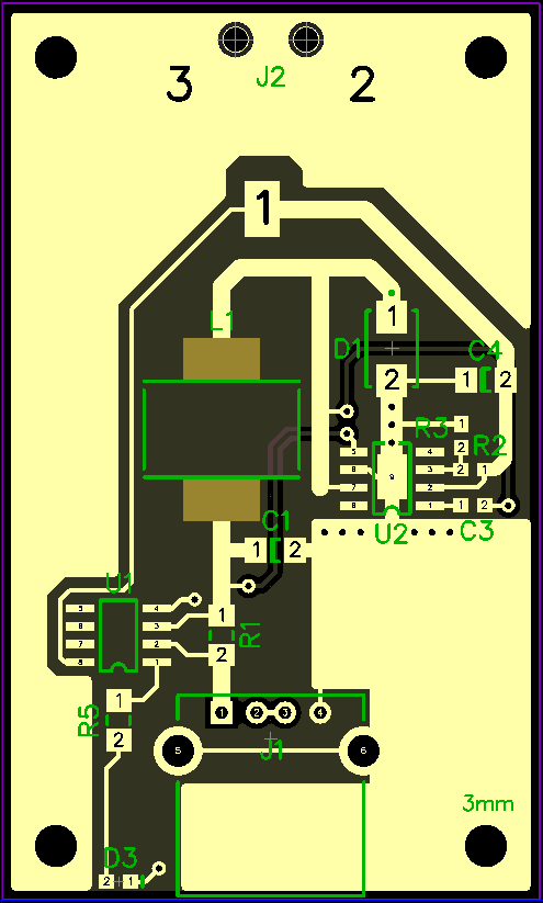
PCB layout for the USB charging port.
Assembly
Eventually I received the components from Digi-Key and the circuit board from OSH Park:
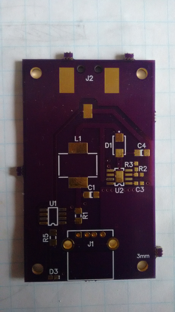
PCB from OSH Park.
Very cool. It has little bits sticking out on the side due to panelization, but they can be broken off and sanded down easily.
Assembly proceeded nicely, with the input DC barrel jack being mounted first, followed by the USB receptacle, the voltage regulator, inductor, diode and most of the resistors and capacitors. I decided to do the current-sensing comparator at a later time as I wanted to test the voltage regulator first.
And then, disaster struck. The regulator would only ever output 0.55V, no matter what I did. I reflowed the components, looked for shorts or cold joints and perused the datasheet for over an hour before my heart sank as I discovered the problem.
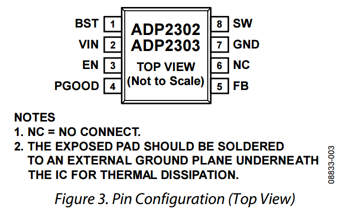
Voltage regulator pin description from the datasheet.
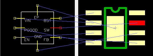
Pin-to-footprint mapping in my PCB layout.
Oops. I think what happened was I forgot to add NC pin 6 to the pin mapping, as a result SW and GND were off by one pad. This is, of course, a complete failure, which in any professional environment would cause the circuit boards to be discarded and the engineer responsible to have a bad day.
In my case I did not want to have to wait another 15-20 days for fixed circuit boards to arrive, so I needed to come up with a fix, and quickly. The trace connecting pin 7 to the switching output rail had to be cut. This can be done easily with any sharp object, if you do this make sure to test continuity to make sure you have completely severed the connection. Then I had to scratch off some solder mask to expose a bit of copper on the switching output rail and put a couple jumper wires to stitch the circuit board (protip: you can use the legs of through-hole resistors as thin wires if you don’t have anything else handy).
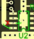
It occurs to me now that since pin 6 was already grounded by my mistake, I could have just shorted pins 6 and 7. At the time I did not realize that though, and decided instead to run a wire under the IC to connect pin 7 to the grounded pad underneath it, causing it to lift slightly. Not a huge problem as it was still thermally connected to the ground plane, but still unsightly. Another alternative would have been an off-board jumper wire from pin 7 to the nearest ground pad, probably one of the barrel jack grounds, but I wanted to avoid unsecured wires floating about.
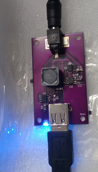
There, I fixed it!
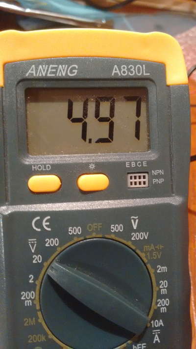
And after that, the regulator finally gave me a stable 5VDC output!
Finally, after assembling the current sensing components, I discovered that this part of the circuit did not actually work (the LED was always on regardless of whether a device was actually plugged into the circuit). I have not yet discovered the cause of this, as when disconnected the output power rail should be high impedance, so no current should flow across it (and hence there should be no voltage drop across the shunt resistor). However, the charger is still serviceable as this was a bonus feature.
Result
I tested the charger on a modern Android smartphone and as expected the phone draws about 1.5 amps at 5V and charges quite fast. The circuit board gets rather hot (not burning hot, but almost uncomfortably so) on the ground plane underneath the regulator, so the thermals could probably be improved quite a lot, but it should work fine when put in an enclosure! Theoretically the regulator can source up to 3 amps but I cannot see the board itself being able to dissipate that much heat; I would expect the regulator to go into thermal shutdown under these conditions.
Success!
It is really cool to be able to design something out of discrete electronic components, check that it works in theory and then have it become a reality as you assemble it. Even if this board was not a great success objectively, I am quite happy it turned out the way it did as I learned a hard lesson about triple-checking the design, and will definitely be making more boards in the future.
comments powered by Disqus