Laser Soldering (Part 1)
I’ve been working on a little side project recently. My goal is to be able to use a laser beam to solder components to circuit boards, in an automated, repeatable fashion using a CNC machine.
It’s mostly for fun; laser soldering does not make sense, even at scale, without very advanced and expensive equipment, and is probably only useful for very small pitch sizes or very temperature-sensitive components, e.g. components that wouldn’t survive or would be damaged by a trip through a reflow oven. But it’s a cool concept nonetheless, and since I wanted to do some laser engraving at home anyway for other purposes, I figured it would be a fun exercise to try and get laser soldering working. And who knows, if it works, it could still come in handy for tiny components that I have trouble soldering by hand.
Setup and Hardware
I acquired a small portable CNC laser engraver from EleksMaker, the “EleksLaser A5 Pro” model. It doesn’t look like much and only provides X and Y control (no Z control), however it is quite cheap for what it is and is fairly well built. One minor complaint I have is that the belts used for motion are hard to tighten and are easily damaged by the fixation mechanism used. If the belt is loose then position control will be inaccurate as the steppers won’t grip the belt. Still, it’s quite good, and comes with the Grbl 0.9j firmware, which can probably be updated to v1.1.
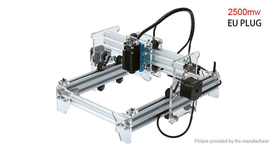
The EleksLaser A5 Pro
The laser module provided is a 445nm 2.5W laser diode encased in a heatsink, with a small fan and a controller board featuring PWM and a “weak laser” button that is useful for positioning. It has a focusing ring to adjust the beam, however like many such laser diodes it uses a cylindrical lens, meaning that it can only focus into a rectangle, not a circle, which is somewhat annoying.
Just because this mode is called “weak laser” doesn’t mean it is safe to look at it with the naked eye, it is still quite strong and can damage your vision if you catch a direct reflection. Under no circumstances should you approach the machine without eye protection while it is powered, as the laser has the potential to go off at any moment.
I also recommend wearing safety goggles with both 445nm and near-infrared (at least 800nm-1200nm) protection, because some laser diodes are frequency-doubled from infrared photons (e.g. 520nm diodes can be frequency-doubled from a 1040nm source) and this IR energy can potentially leak through. I do not believe this is the case for the laser module provided, but there is no easy way to tell by just looking at it. You cannot see infrared radiation nor can your eyes feel it, so you will have no sensory feedback that damage is occurring (until you go blind). Losing vision sucks, so don’t take the chance!
I have set up a small webcam to supervise the device’s operation from a different room. I wanted to mount the webcam on the laser module, however I did not have an easy way to do this (you need a custom mount as the module doesn’t have any helpful mounting points) so currently it is just sitting on the edge of the machine overlooking the work plane at an angle.
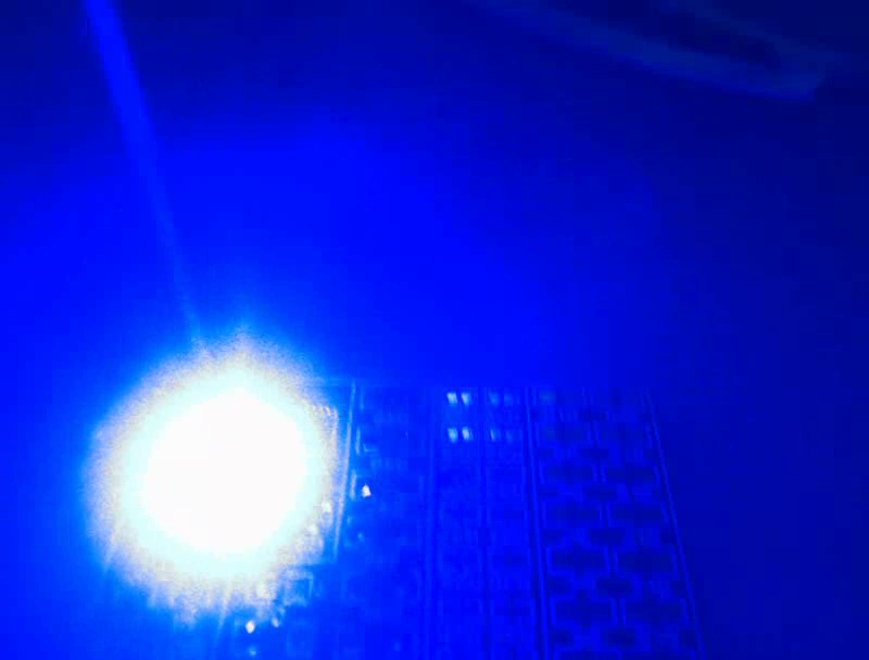
The laser module during operation
First Attempt
I decided to start off with no components, using just solder on a pad, and seeing if I could get solder to flow over the pad and produce a nice shiny-looking joint with Sn63/Pb37 solder paste.
The first try at soldering was a disaster. With no knowledge of how much power would be needed to heat the solder paste to its melting point (I could not find what the absorption coefficient of solder paste is for 445nm light) I had to use trial and error. I started by preparing an array of pads, and aiming the laser at each of them, increasing the power and exposure time for each subsequent pad.
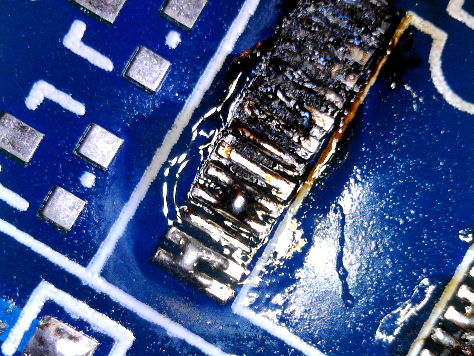
It is clear from observation that the first two pads from the bottom were not heated enough, as the solder did not flow over the entire pad and is not shiny. The third pad shows some promise, but still appears to have insufficiently wetted over the pad. I believe I put too much solder paste for the next two as they look similar to the previous one besides the solder bridge. Every pad after that is burnt, and the later ones were just disintegrated by the beam.
Second Attempt
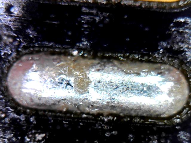
The next attempt was performed on an individual pad (this is a 1.27mm pitch pad, as part of a SOIC28 footprint) with reasonable laser power settings obtained from the previous attempt:
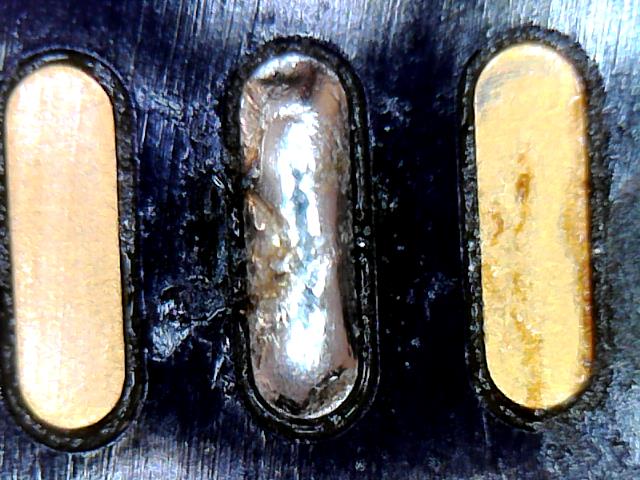
This joint, while showing promise, has at least two major problems:
- the solder didn’t seem to bond at all with the top and bottom edges of the pad
- there are signs of uneven cooling (cracks on the left, top and bottom sides)
I realized that one of the problems I have is that I have very poor beam control on the laser. It is hard to tell what the distribution of optical radiation is across the surface hit by the beam, which is necessary to know about to figure out what you are heating. I suspect most of the energy is imparted in a small area in the center of the beam, and the rest is spread around it, with the energy falling off quickly with distance from the center. This means that even if the beam “appears” from visual inspection to cover the entire pad, it is quite possible that most of the energy is only falling on a small area in the center of the pad, leading to non-uniform heating.
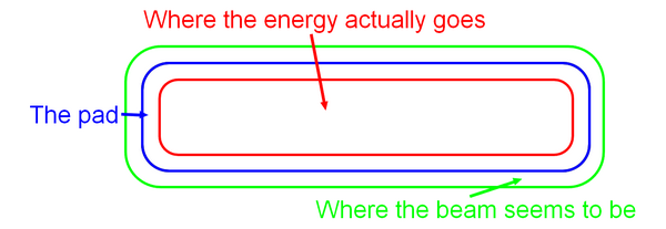
Fortunately, from experimenting a bit it seems that the circuit board withstands the heat from the laser beam quite well, so it is okay to focus the beam to be somewhat wider than the pad. Also, it doesn’t take a lot of power to solder the pad – I was using less than 500mW of optical power in the second attempt – so the beam can be made quite wide with still enough power to work with.
Third Attempt
Having calibrated the laser beam to cover the entire pad with a generous margin, I attempted to address the cooling issue by using the following laser profile: high power for 5 seconds, then gradually reducing the power over a few seconds. My reasoning is that as long as the laser isn’t set to absurd power levels, heating the pad for longer than necessary shouldn’t be an issue and will help bring the entirety of the pad to the same temperature, and I can figure out later what the minimum duration is. Reducing the power gradually should help the solder cool down more gently; after all, with a soldering iron or a hot air gun the board does soak up a lot of heat, but this is not the case with laser soldering, so perhaps this would help avoid cracks?
Aftermath of the third attempt
This joint looks to me quite a lot better than the previous one, there are still visible cracks but the solder has, at last, successfully wet over the entire pad. Perhaps even gentler cooling is needed.
Conclusion
Overall I am quite happy with the results I have gotten so far. It is not usual to using visible light for laser soldering, it seems it is usually done with near-infrared fibre-coupled diodes (e.g. 808nm). This is possibly because you can achieve higher powers with these setups, thus decreasing the exposure time per pad and drastically improving productivity. However from my experiments solder appears to respond positively to 445nm radiation even at low powers.
There is still quite a bit of work in understanding the interaction of the laser beam with the solder paste and the pad, and in calibrating the beam and laser power to achieve a solid, good-quality solder joint, which will hopefully be covered in part 2 of this entry to be posted at a later time.
comments powered by Disqus